Interactive Semiconductor Crystal Structure Simulation
Explore Crystal Lattices, Doping, and Charge Carrier Behavior
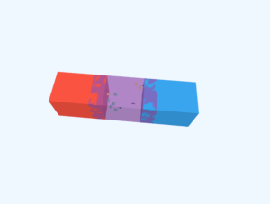
3D Crystal Structure Visualization
Simulation Information
This is a pure (intrinsic) semiconductor crystal. Each atom forms covalent bonds with its four neighbors, creating a stable lattice structure.
How to Use This Simulation
- Select Doping Type: Choose Intrinsic, n-Type, or p-Type using the buttons
- Adjust Doping Level: Move the slider to change dopant concentration (0-100 ppm)
- Modify Temperature: Adjust temperature to see thermal generation effects (250-400 K)
- Rotate the Crystal: Click and drag on the 3D view to rotate and examine the structure
- Observe Changes: Watch carrier counts update and particles move in real-time
Understanding Semiconductor Crystal Structure
What is Semiconductor Crystal Structure?
A semiconductor crystal structure is a highly ordered arrangement of atoms in a repeating lattice pattern. Silicon and Germanium, the most common semiconductors, form diamond cubic structures where each atom bonds covalently with four neighbors. This tetrahedral bonding creates a stable, periodic three-dimensional network that gives semiconductors their unique electrical properties.
Intrinsic Semiconductors
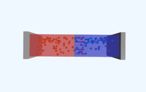
In pure (intrinsic) semiconductors, thermal energy at room temperature breaks some covalent bonds, creating equal numbers of free electrons and holes. The semiconductor crystal structure remains intact, but some electrons gain enough energy to move freely through the lattice. The number of these charge carriers increases exponentially with temperature, following the relationship ni ∝ exp(-Eg/2kT), where Eg is the energy band gap.
n-Type Doping
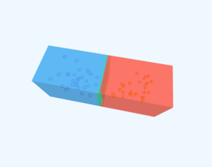
When pentavalent atoms (with 5 valence electrons) like Phosphorus, Arsenic, or Antimony replace silicon atoms in the crystal lattice, they donate extra electrons. These donor atoms fit into the crystal structure but have one "extra" electron that becomes a free charge carrier. This creates an n-type semiconductor where electrons are the majority carriers and holes are minority carriers.
p-Type Doping
When trivalent atoms (with 3 valence electrons) like Boron, Aluminum, or Indium replace silicon atoms, they create holes in the crystal structure. These acceptor atoms are missing one electron to complete the tetrahedral bonding, creating a hole that can accept an electron. This forms a p-type semiconductor where holes are majority carriers and electrons are minority carriers.
Temperature Effects
Higher temperatures provide more thermal energy to the crystal lattice, increasing the rate of covalent bond breaking. This generates more electron-hole pairs intrinsically, increasing conductivity. At very high temperatures, the intrinsic carrier concentration can exceed the doping concentration, causing the semiconductor to behave more like an intrinsic material regardless of doping.
Key Concepts
- Crystal Lattice: Periodic 3D arrangement of atoms with long-range order
- Covalent Bonding: Each silicon atom shares electrons with four neighbors
- Charge Carriers: Free electrons (negative) and holes (positive)
- Doping Concentration: Number of dopant atoms per unit volume (measured in ppm or cm⁻³)
- Carrier Mobility: How easily charge carriers move through the crystal
- Recombination: Process where electrons and holes combine, releasing energy
Real-World Applications
Transistors
Building blocks of all modern electronics, using controlled doping to create switching and amplification devices.
Integrated Circuits
Billions of transistors on a single chip, made possible by precise control of crystal structure and doping.
Solar Cells
Convert light to electricity using p-n junctions formed by differently doped regions in the crystal.
LEDs
Light emission from electron-hole recombination in specially engineered semiconductor crystals.
Sensors
Temperature, light, and pressure detection using changes in semiconductor electrical properties.
Power Electronics
Efficient energy conversion and control using heavily doped semiconductor devices.