PN Junction Diode Reverse Bias Simulation
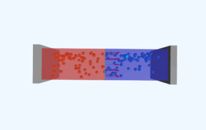
This simulation demonstrates the behavior of a PN junction diode under reverse bias conditions. When reverse biased (n-side positive, p-side negative), the depletion region widens and barrier potential increases (V₀ + V), suppressing diffusion current. Only a small drift current flows due to minority carriers being swept across the junction.
Value: 0 V
Value: 300 K
P-type (Acceptors)
N-type (Donors)
Depletion Region
Electrons
Holes
Current Flow