Interactive p-n Junction Simulation
Explore Semiconductor Physics Through 3D Visualization
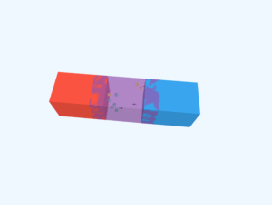
3D Simulation Interface
How to Use This Simulation
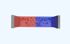
- Adjust Bias Voltage: Move the voltage slider left (negative) for reverse bias or right (positive) for forward bias
- Observe Changes: Watch the depletion region width change and charge carriers move
- Change View Angle: Use the angle slider to rotate the simulation
- Interactive 3D: Click and drag on the canvas to rotate, scroll to zoom in/out
Understanding the p-n Junction Simulation
What is a p-n Junction?
A p-n junction forms when p-type semiconductor (with excess holes as majority carriers) and n-type semiconductor (with excess electrons as majority carriers) are joined together. This junction is the fundamental building block of most semiconductor devices.
The Depletion Region
At the junction interface, electrons from the n-type region diffuse into the p-type region and recombine with holes, while holes from the p-type region diffuse into the n-type region. This process creates a depletion region — an area depleted of mobile charge carriers but containing fixed ions. These ions create an electric field that opposes further diffusion.
Effects of Bias Voltage
- Forward Bias (Positive Voltage): Applying positive voltage to the p-type side reduces the built-in electric field, shrinking the depletion region. This allows charge carriers to flow easily, enabling current conduction.
- Reverse Bias (Negative Voltage): Applying negative voltage to the p-type side increases the electric field, expanding the depletion region. This blocks current flow, with only a tiny leakage current present.
- Equilibrium (Zero Bias): With no external voltage, the junction reaches equilibrium with a stable depletion width determined by the material properties.
Key Concepts
- Charge Carriers: Electrons (negative) in n-type and holes (positive) in p-type materials
- Built-in Potential: Natural voltage barrier created by the depletion region (~0.7V for silicon)
- Current Flow: Requires forward bias to overcome the built-in potential barrier
Real-World Applications
Rectifier Diodes
Convert alternating current (AC) to direct current (DC) in power supplies
Solar Cells
Convert light energy into electrical energy through the photovoltaic effect
LEDs
Emit light when forward biased, used in displays, lighting, and indicators
Transistors
Amplify and switch electronic signals using multiple p-n junctions