Enhanced Transistor Switching Simulation
Circuit Diagram
Transfer Characteristic
Waveforms
0.0 V
Cutoff (<0.6V)
Active (0.6V-2.8V)
Saturation (>2.8V)
100 kΩ
1.0 kΩ
250
Circuit Parameters
Base Current (IB)
0.0 μA
Collector Current (IC)
0.0 mA
Output Voltage (VCE)
5.0 V
Power Dissipation
0.0 mW
State: Cutoff
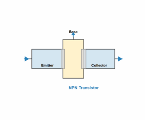
Transistor Switching Characteristics
This simulation demonstrates the operation of an NPN transistor in a common-emitter configuration as a switch. The transistor transitions between three distinct regions of operation based on the input voltage (VBB):
// Cutoff Region (VBB < 0.6V):
IB ≈ 0, IC ≈ 0, VCE ≈ VCC
// Active Region (0.6V ≤ VBB ≤ 2.8V):
IB = (VBB - 0.6V)/RB
IC = β × IB
VCE = VCC - IC × RC
// Saturation Region (VBB > 2.8V):
VCE ≈ 0.2V, IC ≈ VCC/RC
IB ≈ 0, IC ≈ 0, VCE ≈ VCC
// Active Region (0.6V ≤ VBB ≤ 2.8V):
IB = (VBB - 0.6V)/RB
IC = β × IB
VCE = VCC - IC × RC
// Saturation Region (VBB > 2.8V):
VCE ≈ 0.2V, IC ≈ VCC/RC
The example values demonstrate a typical switching application where the transistor changes from fully off (cutoff) to fully on (saturation) as the input voltage increases beyond the threshold. The active region provides amplification but is typically minimized in switching applications.