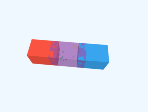
3D p-n Junction Diode Simulation
p-n Junction Diode Operation
A semiconductor diode is a p-n junction with metallic contacts at both ends. When forward biased (positive voltage on p-side), the depletion region narrows and current flows easily. When reverse biased, the depletion region widens and minimal current flows.
In this simulation, adjust the voltage slider to see how the depletion region changes and how electrons (blue spheres) and holes (orange spheres) move across the junction. The current display shows the resulting current flow.
Physics Details:
Depletion Region: The gray area where mobile charge carriers (electrons and holes) are depleted, leaving behind fixed ions that create an electric field.
Forward Bias: Applied voltage reduces the built-in potential, allowing majority carriers to flow across the junction (electrons from n to p, holes from p to n).
Reverse Bias: Applied voltage increases the built-in potential, widening the depletion region and preventing current flow (except for tiny minority carrier currents).
Current Flow: Notice how current increases exponentially with forward bias but remains nearly zero with reverse bias.