PN Junction Forward Bias Simulation
Visualizing semiconductor behavior under forward bias conditions
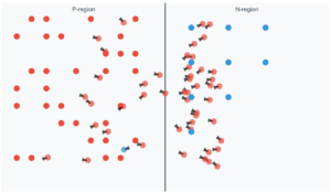
This interactive simulation demonstrates how applying a forward bias voltage to a PN junction lowers the potential barrier, enabling current flow. Adjust the voltage slider to observe the dynamic changes in the depletion region and charge carrier movement.
0.00 V
0V (no bias) → 1V (full forward bias)
PN Junction Theory: Forward Bias
•
Forward bias occurs when the P-type is connected to the positive terminal and N-type to negative, reducing the potential barrier.
•
The applied voltage opposes the built-in potential, narrowing the depletion region and lowering the energy barrier.
•
Majority carriers (holes in P-type, electrons in N-type) gain enough energy to cross the junction.
•
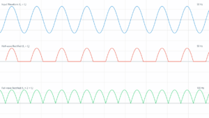
Current increases exponentially with voltage according to the diode equation: I = I₀(e^(qV/kT) - 1).