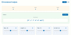
3D p-n Junction Simulation
Visualizing Semiconductor Interface Challenges
This interactive simulation demonstrates why physically joining p-type and n-type semiconductor slabs cannot create a proper p-n junction due to surface roughness at the atomic level (~2-3Å). Explore how microscopic irregularities affect semiconductor interfaces.
Initializing 3D simulation...
Simulation Controls
Example
Question:
Can we take one slab of p-type semiconductor and physically join it to another n-type semiconductor to get a p-n junction?
Solution:
No! Any slab, however flat, will have roughness much larger than the inter-atomic crystal spacing (\(\sim 2\) to \(3\,\text{\AA}\)), so continuous contact at atomic level is not possible. The junction behaves as a discontinuity for flowing charge carriers.
Key Concepts
Surface Roughness Challenge: Real semiconductor surfaces have roughness much larger than inter-atomic spacing (2-3Å), preventing continuous contact at the atomic level needed for a proper p-n junction.
Manufacturing Reality: Even with "flat" surfaces, microscopic irregularities create discontinuities that disrupt charge carrier flow and prevent proper junction formation.
Performance Tips
- Use "Low" roughness setting for better performance on older devices
- Reduce zoom level when viewing atomic structure
- Pause animation when not actively interacting with the simulation